

As the demand for semiconductors continues to grow, the semiconductor industry has been investing in capital project construction to keep up with the ever-increasing demand. The construction of fabrication plants, also known as "fabs," is a critical step in the production process, and the industry is no stranger to large-scale construction projects.
However, the complexity of the manufacturing process and the specialized nature of the construction process pose unique challenges, particularly in finding skilled labor for the construction of the semiconductor fabs.
In this blog post, we will explore the developments in capital project construction in the semiconductor fabrication sector and the challenges faced by the industry in finding skilled labor.
- Background on the Semiconductor Fabrication Space
- Challenges
- Developments in Semiconductor Fab Construction
The semiconductor industry has been driving technological advancement across the world for many decades. Semiconductors, the building blocks of modern electronic devices, have seen a tremendous surge in demand in recent years, particularly due to the rise of smart devices, automated machines, the Internet of Things (IoT), Industry 4.0, and the increasing reliance on technology in our daily lives. As the demand for semiconductors continues to grow, the industry has been investing heavily in capital project construction to meet the demand.
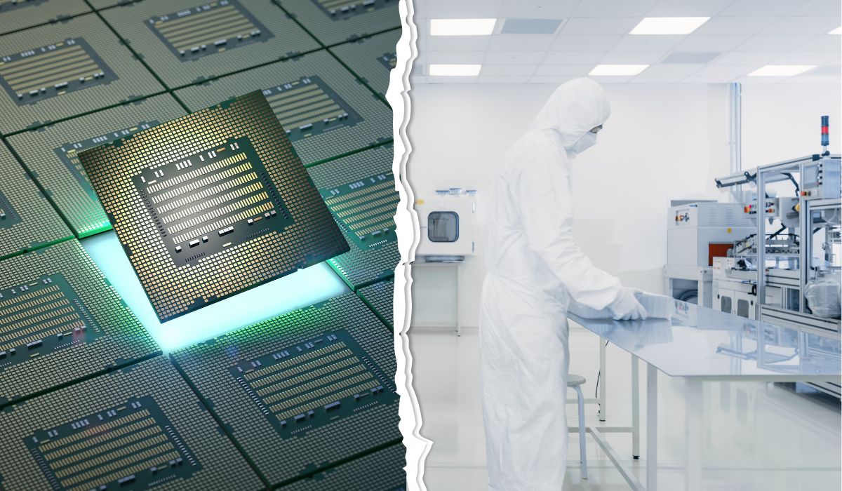
In the semiconductor fabrication space, the construction of fabrication plants, also known as "fabs," is a critical step in the production process. These facilities require a significant investment in capital, and they must be built to exacting standards to ensure that the delicate and complex manufacturing process can take place.
The manufacturing process involves the use of specialized tools, clean rooms, and power and cooling systems. As a result, the construction of semiconductor fabs is a complex and costly process that requires specialized expertise. The semiconductor industry is no stranger to large-scale construction projects, and as the demand for semiconductors continues to grow, so too does the need for new fabs.

Challenges
Facilities must be built to incredibly high standards of cleanliness and precision
The construction of semiconductor fabs presents several unique challenges. First, the facilities themselves must be built to incredibly high standards of cleanliness and precision, as even the tiniest particle or variation in temperature can disrupt the manufacturing process. The complexity of the manufacturing process also means that fabs require significant investment in infrastructure, including specialized engineering and tools, clean rooms, and power and cooling systems.
Finding skilled labor for semiconductor fab construction
One of the most significant challenges faced by the semiconductor industry in capital project construction is finding skilled labor. The specialized nature of the construction process means that workers require specific training and expertise to work on the project. In recent years, the semiconductor industry has struggled to find enough skilled workers to meet the demand for construction projects, leading to delays and increased costs.
The issue of finding skilled labor is not unique to the semiconductor industry. According to the Bureau of Labor Statistics, the construction industry as a whole is facing a skilled labor shortage. As a result, the semiconductor industry has been investing in training and education programs to help develop the skilled workforce needed for construction projects. This includes partnerships with universities and technical schools to provide training in specialized areas such as clean room construction and semiconductor manufacturing
Developments in Semiconductor Fab Construction
To address these challenges, the semiconductor industry has been investing in new technologies and processes to improve the efficiency and effectiveness of capital project construction. These developments include:
Building Information Modeling (BIM)
One of the most significant developments in capital project construction in the semiconductor fabrication sector is the use of building information modeling (BIM) technology.
Civil and construction engineers in some companies are utilizing advanced digital tools, such as BIM, to create detailed 3D models of the fab before construction begins. BIM can help identify potential issues and challenges early in the process, reducing delays and costs. BIM can also help with the ongoing operation and maintenance of the fab, by providing detailed information on the various systems and components of the facility.
Prefabrication
Prefabrication involves the manufacture of building components off-site, which are then assembled on-site. Structural engineers facilitate this process which help reduce the amount of time and labor required for on-site construction, and can also improve quality control by ensuring that components are manufactured to exacting standards. Prefabrication design by structural engineers can also reduce waste, as materials can be optimized for specific components.
Modularization
Modularization involves the use of pre-fabricated building components that are assembled on-site to create the final facility. Modular construction involves building components off-site in a controlled environment, which can then be assembled on-site. This approach reduces the amount of time spent on construction and can also reduce costs.
Modularization can help reduce construction time and costs, as the components are manufactured off-site and shipped to the construction site for assembly. Modularization can also improve quality control, as the components are manufactured to exacting standards.
Development of new technologies
The industry is also investing in new technologies for the manufacturing process itself. For example, advanced lithography machines can now produce transistors on a much smaller scale, leading to faster and more powerful processors. The development of new manufacturing technologies has a direct impact on capital project construction, as the fabs must be built to accommodate these new machines.
Training and education programs
The semiconductor industry is investing in training and education programs to help develop the skilled workforce needed for construction projects. This includes partnerships with universities and technical schools to provide training in specialized areas such as clean room construction and semiconductor manufacturing processes. These programs can help ensure that there is a steady supply of skilled workers to meet the growing demand for construction projects.
ParFab's Capital Construction Services
ParFab Companies’ Capital Construction Services combines the efficiency, safety, and quality of in-house contracting with the extensive resources of our corporate strength. From large capital projects to emergency services, we offer a complete package of construction services from start to finish.
- Structural Steel Fabrication
- Equipment – Setting, Assembly & Alignment
- ASME Code Welding
- Planning and Scheduling
- Project and Cost Controls
- Estimating and Budgeting
- Field Work Execution
- Procurement
- Subcontractor Management
- Piping
- HVAC
